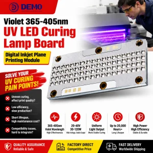
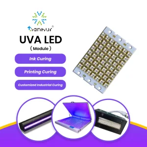
Osaka serves as the economic hub of western Japan, boasting a highly concentrated ecosystem of precision engineering, medical device manufacturing, advanced electronics, and commercial printing. In the contemporary manufacturing landscape of the Keihanshin Metropolitan Area, there has been a significant shift from traditional thermal or mercury vapor curing methods toward solid-state UV LED 3D printing curing systems. This transition is motivated by stringent environmental regulations, the pursuit of zero-defect quality standards, and the imperative to minimize thermal stress on delicate polymers.
High-performance 3D printing, especially SLA, DLP, and LCD photopolymerization systems used in medical, dental, and tooling sectors in Osaka, requires uniform ultraviolet radiation to guarantee precise mechanical properties. Variations in curing light uniformity lead to internal stresses, warp defects, and inconsistent polymer conversion. Our customizable UV LED systems are designed to address these concerns. They supply target-specific wavelengths (typically 365nm to 405nm) with industrial-grade irradiance stability, meeting the high demands of Osaka's top-tier manufacturers.
On a global scale, the industrial curing market is undergoing a transition driven by smart automation and sustainability goals. The international shift to UV LED curing technology is accelerated by the Minamata Convention on Mercury, forcing industries to phase out conventional mercury arc lamps. At the same time, the emergence of Industry 4.0 demands intelligent curing engines that communicate directly with factory PLCs.
Our latest UV LED product portfolio integrates real-time optical feedback, internal thermal sensing, and closed-loop current control. These features ensure that the radiant flux remains constant over an operating life exceeding 30,000 hours. This degree of control is crucial for automotive assembly, advanced optics bonding, and mass-scale 3D printing, where process variability translates directly to operational losses.
The efficiency of UV curing is dictated by the match between the emission spectrum of the UV light source and the absorption profile of the photoinitiators within the resin. Most industrial resins formulated for SLA, DLP, and LCD 3D printing contain photoinitiators like TPO or BAPO, which show high reactivity profiles around the 385nm and 405nm wavelengths.
Conversely, surface curing and micro-feature replication benefit significantly from the higher photon energy of shorter wavelengths, such as 365nm. This energy is essential to overcome oxygen inhibition at the liquid-resin interface. By employing dual-wavelength and multi-wavelength architectures within our COB (Chip-on-Board) modules, Dongguan LumiCure Light Co., Ltd. allows engineers in Osaka to achieve balanced polymer cross-linking. This approach delivers hard, tack-free surfaces along with fully developed, deep structural cure properties.
Technical Insight: Integrating multi-chip arrays on custom metal-core PCBs enables our systems to emit co-axial 365nm and 405nm spectrums from a single optical aperture. This design eliminates the shadow effects and uneven curing patterns associated with separate multi-lamp configurations.
Our UV LED curing technology is tailored to address the unique needs of Osaka's core manufacturing sectors:
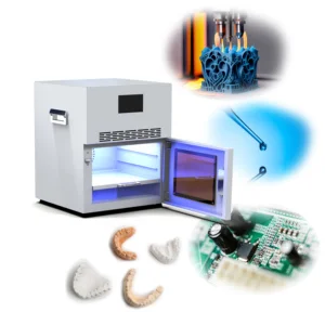
Providing highly uniform 405nm light boxes and spot systems to medical clinics and orthodontic labs across Osaka for fabricating biocompatible dental crowns, surgical guides, and customized prosthetics.
Our high-power 365nm and 395nm LED systems are used for solder mask curing, conformal coating, and optical micro-bonding in Osaka's prominent electronics manufacturing centers.
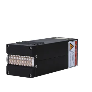
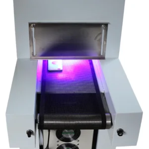
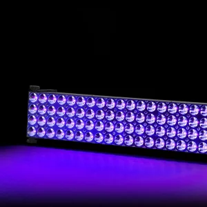
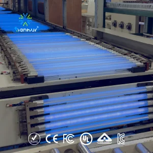
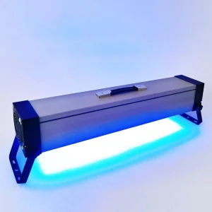
Integrating conveyor-compatible high-power UV light bars into regional printing lines, maximizing throughput while reducing heat transmission onto thin plastic substrates.
Dongguan LumiCure Light Co., Ltd. is a professional China UV LED curing lamp manufacturer specializing in the research, development, production, and supply of industrial UV curing systems and customized UV LED solutions. With a strong focus on innovation, quality, and customer satisfaction, LumiCure has become a trusted partner for manufacturers worldwide seeking efficient and reliable curing technologies.
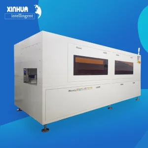
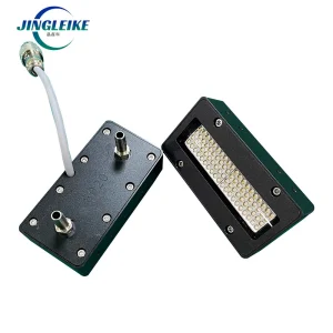
Our product range includes UV LED curing lamps, UV LED spot curing systems, flood curing lamps, conveyor UV curing machines, UV LED modules, printing curing systems, adhesive curing equipment, and customized industrial UV solutions. These products are widely applied in printing, electronics assembly, semiconductor packaging, optical bonding, automotive manufacturing, medical devices, 3D printing, and various precision industrial processes.
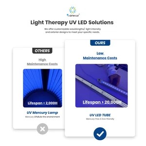
Backed by an experienced engineering team and advanced manufacturing facilities, LumiCure is committed to developing energy-saving and environmentally friendly UV curing technologies. Our products feature high curing efficiency, precise wavelength output, long service life, low maintenance requirements, and intelligent control capabilities, helping customers improve productivity while reducing operating costs.
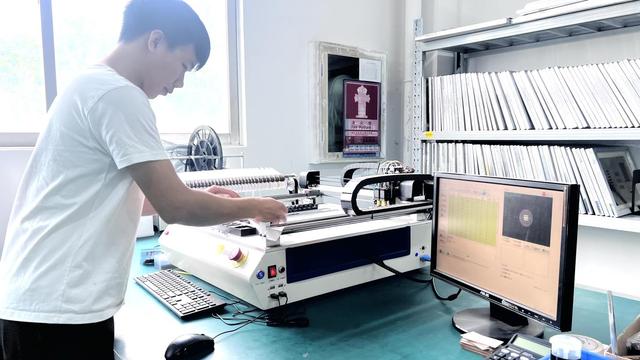
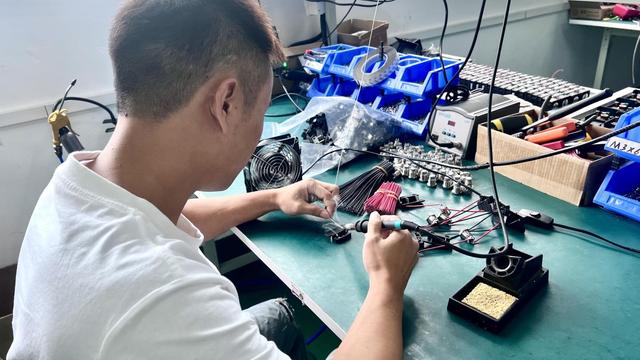
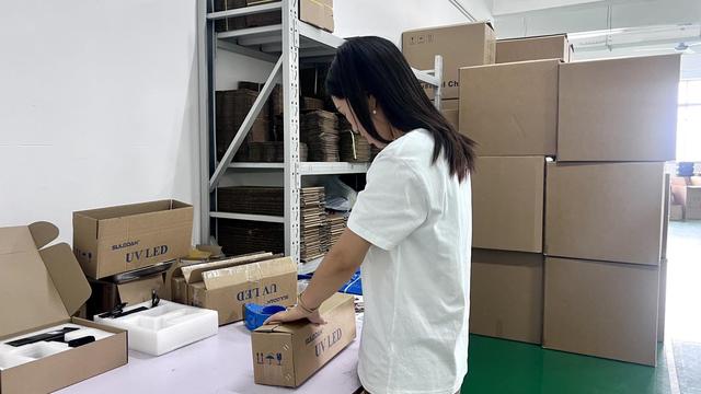
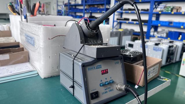
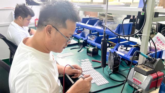
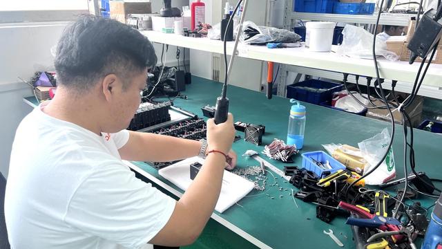
Quality remains the foundation of our business. Every product undergoes rigorous testing and strict quality control procedures throughout the manufacturing process to ensure consistent performance and reliability. We also provide comprehensive OEM and ODM services, enabling customers to customize products according to their specific technical and application requirements.
Serving clients across Europe, North America, Asia, the Middle East, and other global markets, Dongguan LumiCure Light Co., Ltd. continues to deliver innovative UV LED curing solutions that support sustainable and efficient industrial manufacturing.
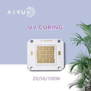
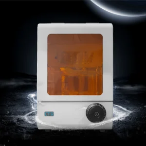
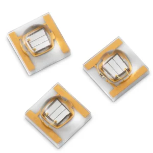
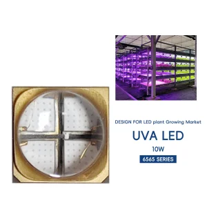
As UV LED power densities rise, the management of thermal energy within the LED junction becomes a critical engineering challenge. The optical output efficiency of UV LEDs is lower than that of blue LEDs used for visible lighting; approximately 55% to 70% of the electrical energy supplied to a UV LED chip is converted into heat. Without proper thermal management, the junction temperature will rise, causing a decrease in optical power output, shifts in emission wavelength, and premature diode degradation.
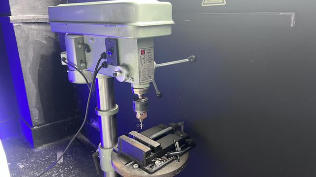
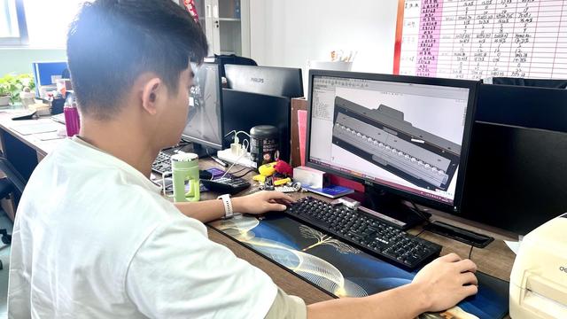
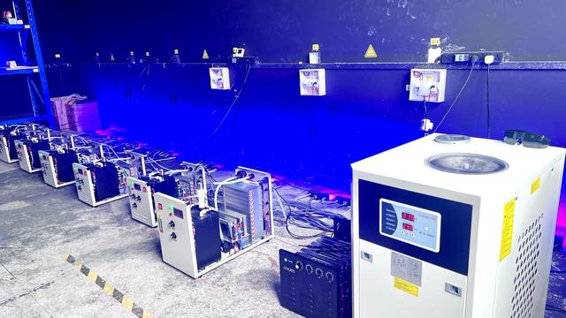
Our manufacturing facility uses high-conductivity copper substrates combined with direct-die attach eutectic bonding processes. This approach reduces thermal resistance down to less than 0.5°C/W. For air-cooled configurations, micro-channel extruded aluminum heatsinks and variable-speed fans are integrated to maintain steady junction temperatures during continuous high-intensity curing. For ultra-high irradiance applications (exceeding 16 W/cm²), water-cooled manifolds maintain the LED junction temperature within optimal limits. This helps ensure consistent curing results across large production runs, which is particularly beneficial for high-throughput lines operated by manufacturers in Osaka.
Furthermore, our digital drivers feature integrated PWM interfaces that support precise duty cycle tuning. This control is critical for preventing thermal buildup during high-frequency micro-exposure cycles, which are common in precision DLP 3D printing.
 LumiCure Light