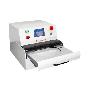
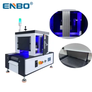
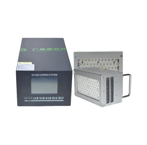
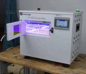
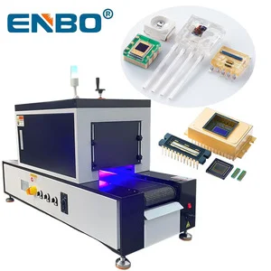
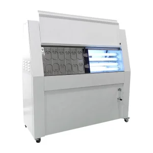
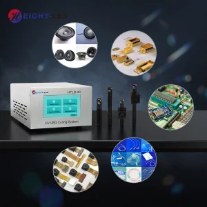
Explore our highly integrated UV LED curing chambers, aging test systems, and spot/flood radiation setups designed for industrial manufacturing lines.
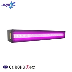
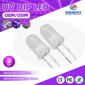
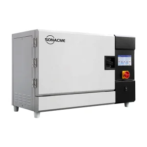
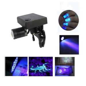
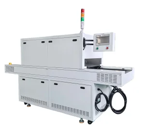
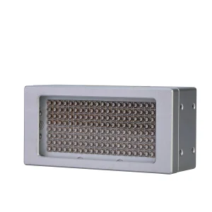
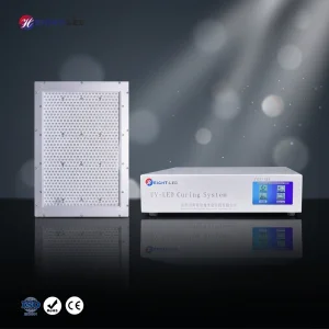
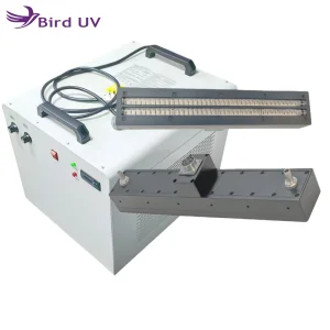
Dongguan LumiCure Light Co., Ltd. is a professional China UV LED curing lamp manufacturer specializing in the research, development, production, and supply of industrial UV curing systems and customized UV LED solutions. With a strong focus on innovation, quality, and customer satisfaction, LumiCure has become a trusted partner for manufacturers worldwide seeking efficient and reliable curing technologies.
Our product range includes UV LED curing lamps, UV LED spot curing systems, flood curing lamps, conveyor UV curing machines, UV LED modules, printing curing systems, adhesive curing equipment, and customized industrial UV solutions. These products are widely applied in printing, electronics assembly, semiconductor packaging, optical bonding, automotive manufacturing, medical devices, 3D printing, and various precision industrial processes.
Quality Assurance: Backed by an experienced engineering team and advanced manufacturing facilities, LumiCure is committed to developing energy-saving and environmentally friendly UV curing technologies. Our products feature high curing efficiency, precise wavelength output, long service life, low maintenance requirements, and intelligent control capabilities.
Undergoing a major shift towards solid-state narrowband irradiation systems, the semiconductor fabrication process demands unparalleled thermal control and uniform UV illumination.
Traditional mercury vapor systems emit broad spectrums causing thermal stress on delicate wafers. Modern optical systems employ monochromatic 365nm, 385nm, 395nm, and 405nm LED engines, targeting specific photoinitiator absorption bands in modern wafer dicing tapes and optical adhesives without unnecessary infrared emission.
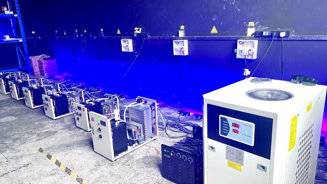
Due to the close proximity of light sources to semiconductor dies, thermal dissipation is a vital engineering priority. High-output chillers (both air-cooled and water-cooled) maintain thermal equilibrium, protecting substrate integrity and preventing optical drift in LED modules during long production cycles.
Oxygen inhibition frequently leads to tacky surface curing in sub-micron bonding layers. Integrating nitrogen (N2) gas purging systems within the curing chamber displaces oxygen, accelerating the polymerization process of optical adhesives (like OCA) and ensuring zero surface tackiness.
Future Engineering Horizon: The industry is moving towards smart curing systems equipped with in-situ radiometers. These systems dynamically adjust output power based on real-time feedback loops, ensuring that every square millimeter of the wafer receives consistent UV dosage, matching the requirements of next-generation 3D IC packaging and chiplets.
From back-end wafer processing to optical communication module packaging, high-precision UV LED curing is the backbone of yield optimization.
During wafer dicing and grinding, temporary adhesive tapes are used to secure wafers. Wafer film degumming equipment utilizes targeted ultraviolet light to weaken the adhesive strength of UV-release tapes, allowing clean peeling without leaving chemical residue. Our 8-inch and 12-inch UV LED curing ovens provide uniform radiation, facilitating high-throughput wafer processing for semiconductor foundries.
Laminating AR/VR optical lenses and high-resolution display panels requires minimal thermal expansion. Our quad-wavelength N2 inert gas curing chambers are tailored for OCA (Optically Clear Adhesive) laminating, providing uniform, shrink-controlled, and bubble-free bonding under controlled gas atmospheres.
Active alignment of optical fibers, transceivers, and silicon photonics relies on sub-micron alignment accuracy. Multi-channel UV LED spot curing systems deliver precise light spot sizing to fast-cure specialized epoxies instantly, locking optical components in place without physical shifting or misalignment.
Protecting wire bonds and sensitive micro-components involves applying UV-curable glob tops and encapsulants. Conveyor-based or benchtop ultraviolet curing units ensure fast processing of high-density printed circuit boards (PCBs), providing robust environmental protection against humidity, dust, and mechanical impact.
How LumiCure leverages Dongguan's manufacturing ecosystems to deliver cost-competitive, high-reliability industrial UV systems.
Situated in Dongguan, the heart of Southern China's advanced electronics and machinery hub, Dongguan LumiCure Light Co., Ltd. benefits from a highly integrated local supply chain. We maintain direct access to raw materials, including custom-grown high-quality epitaxial wafers, precision quartz lens optics, and heavy-duty thermal-management aluminum profiles. This localized cluster allows us to compress the engineering cycle from prototype design to full-scale production, offering short lead times for international orders.
Our commitment to Industry 4.0 principles includes digital tracking of components, precise calibration tools, and cleanroom assembly zones for sensitive optical arrays. For our international clients, this translates into consistent quality, batch-to-batch repeatability, and a secure supply chain that minimizes the risks of shipping delays or performance deviations.
Unlike legacy mercury systems, UV LED units operate mercury-free and produce zero ozone during curing, aligning with global environmental directives such as RoHS and WEEE.
We streamline industrial integration by designing products that match global electrical, mechanical, and safety standards.
Our systems support universal input voltages (e.g., 110V/220V/380V) and are designed with standard industrial communication protocols such as RS485, Modbus, and EtherNet/IP. This simplifies integration into automatic pick-and-place lines and robotic arms.
We provide tailormade optical profiles, including line light sources, large area spot systems, and circular ring setups. Using specialized quartz arrays, we optimize the illumination angle to maximize irradiance uniformness across varying target heights.
Semiconductor fabrication demands strict particulate control. LumiCure's high-performance equipment features fanless, water-cooled configurations and anodized aluminum enclosures that prevent outgassing, ensuring compatibility with Class 10 and Class 100 cleanrooms.
Every product is backed by comprehensive technical documentation, compliance certificates, and expert after-sales support.
Dongguan LumiCure Light Co., Ltd. provides robust technical support throughout the procurement cycle. We supply complete CAD and 3D modeling files to assist with mechanical integration, as well as spectral reports and radiometric calibration data for process qualification.
Our experienced engineering team is available to assist with custom optical calculations, adhesive testing, and thermal evaluations. We offer OEM/ODM services to adapt our systems to your specific manufacturing workflow, ensuring optimal performance and compatibility with your materials.
Get detailed technical answers regarding system integration, wavelength matching, and equipment selection.
Browse our selection of specialized wafer degumming chambers, inert gas laminating systems, and micro-component UV lights.
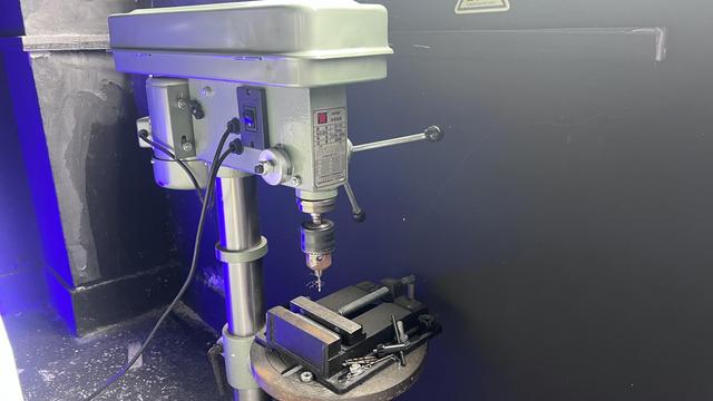
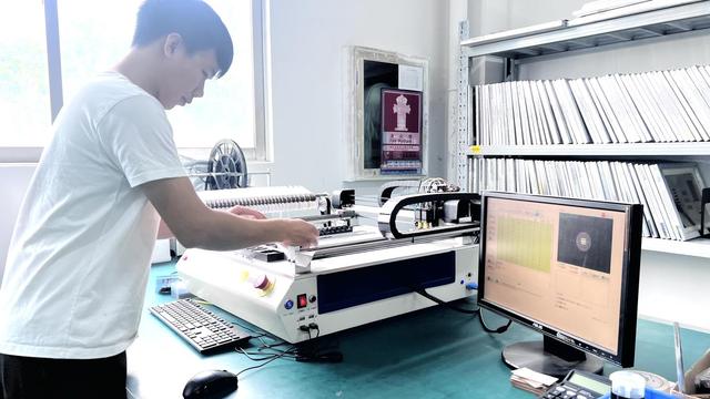
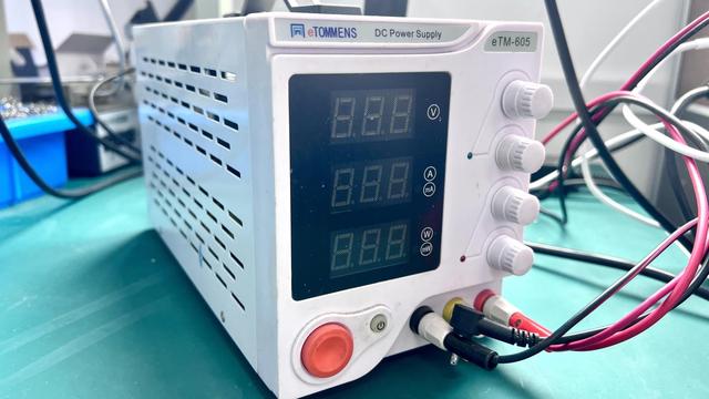
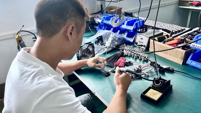
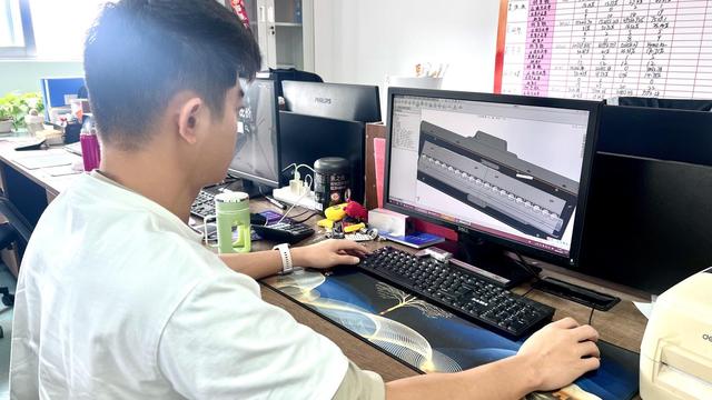
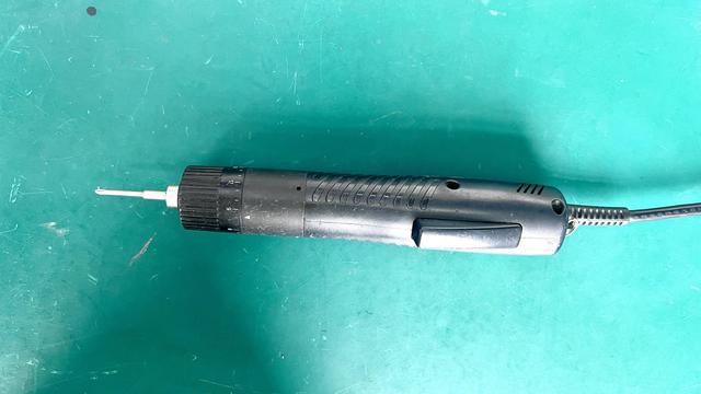
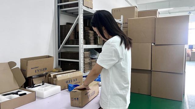
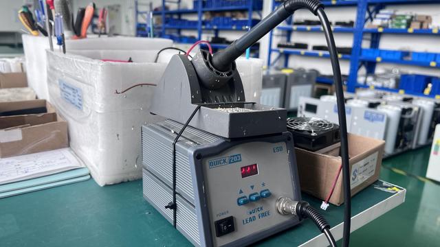
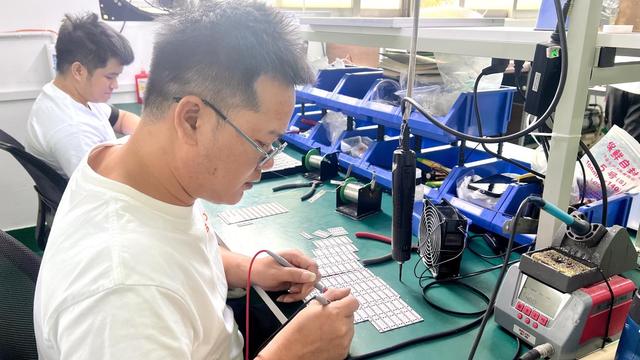
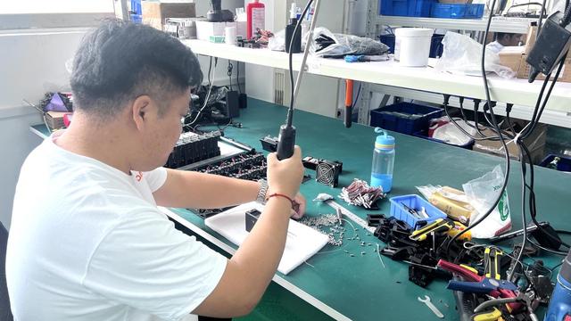
Inside LumiCure: Take a look at our advanced production lines, testing laboratories, and precision manufacturing capabilities in Dongguan, China.
 LumiCure Light