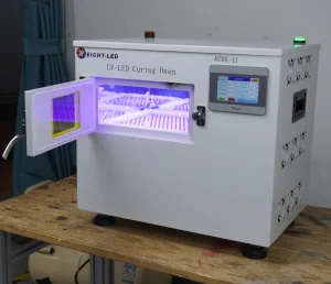
Engineered for high-precision components, advanced electronics assembly, and simulation testing in the Peruvian industrial marketplace.
The industrial economy of Peru is undergoing a major paradigm shift. Historically centered on primary resource extraction, the Peruvian manufacturing sector is rapidly diversifying into localized, high-value manufacturing, electronics assembly, and optoelectronic instrumentation. Key technical hubs in Lima, Arequipa, and Callao are driving the domestic development of specialized telemetry sensors for mining safety, structural health monitoring, and smart agricultural networks.
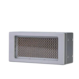
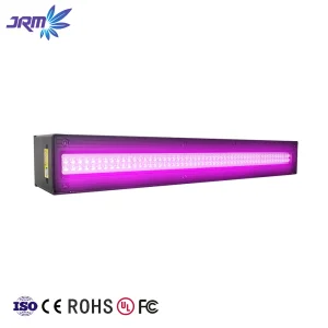
To manufacture these telemetry sensors, local assemblers must rely on precision micro-electronics and protective coatings. Traditional thermal curing or mercury arc lamps fall short due to excessive heat emission, which can damage delicate micro-sensors and silicon substrates. This is where UV LED Semiconductor Curing Systems become critical. By delivering localized, high-intensity ultraviolet irradiation at narrow-band wavelengths (primarily 365nm and 395nm), Peruvian manufacturers can cure adhesives instantly without imparting thermal stress to electronic packages.
On a global scale, the semiconductor industry is moving towards advanced 3D packaging, Wafer-Level Chip-Scale Packaging (WLCSP), and high-density System-in-Package (SiP) structures. These technologies require exceptional precision in the optical alignment and mechanical stabilization of die structures before final encapsulation. Traditional ovens take hours and consume massive floor space; UV-curable polymers, when activated by high-power LED systems, achieve cross-linking in under three seconds.
Unlike legacy mercury lamps that emit broad-band spectra (including IR and UVC wavelengths that degrade substrates), modern UV LED heads emit pure, monochromatic light. Engineering teams specify 365nm for deep penetration into optical adhesives, 395nm for high-speed surface curing of thick coatings, and 405nm for sensitive plastic matrices. This precise control over optical wavelengths ensures minimal thermal dissipation, making it suitable for thin-wafer processing and flexible electronics.
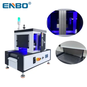
A common challenge in semiconductor optical bonding is oxygen inhibition. Ambient oxygen molecules terminate the free radicals necessary for acrylic and epoxy polymerization, resulting in a sticky, under-cured surface layer. Modern production lines in the semiconductor and display fields (like OCA laminating) now integrate enclosed curing chambers filled with Nitrogen (N2). Displacing oxygen down to less than 100 ppm allows the curing process to achieve 100% polymer conversion, ensuring high chemical resistance and mechanical shear strength.
Sealing telemetry components, strain gauges, and geo-technical micro-sensors against moisture, vibration, and dust ingress. High-intensity spot UV systems quickly cure protective acrylic and polyurethane coatings directly on the electronics assembly line.
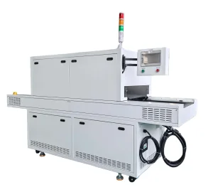
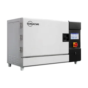
Peruvian material research universities and custom micro-electronics firms utilize benchtop wafer film degumming ovens. These ovens apply highly uniform UV exposure to neutralize adhesive tape grip, enabling clean die singulation without stress.
Given Peru's diverse climate zones—from high UV Andes plateaus to humid coastal areas—manufacturers of protective paints, solar modules, and automotive parts use accelerated weathering chambers to simulate solar UV degradation.
Dongguan LumiCure Light Co., Ltd. is a professional China UV LED curing lamp manufacturer specializing in the research, development, production, and supply of industrial UV curing systems and customized UV LED solutions. With a strong focus on innovation, quality, and customer satisfaction, LumiCure has become a trusted partner for manufacturers worldwide seeking efficient and reliable curing technologies.
Our product range includes UV LED curing lamps, UV LED spot curing systems, flood curing lamps, conveyor UV curing machines, UV LED modules, printing curing systems, adhesive curing equipment, and customized industrial UV solutions. These products are widely applied in printing, electronics assembly, semiconductor packaging, optical bonding, automotive manufacturing, medical devices, 3D printing, and various precision industrial processes.
Backed by an experienced engineering team and advanced manufacturing facilities, LumiCure is committed to developing energy-saving and environmentally friendly UV curing technologies. Our products feature high curing efficiency, precise wavelength output, long service life, low maintenance requirements, and intelligent control capabilities, helping customers improve productivity while reducing operating costs.
Quality remains the foundation of our business. Every product undergoes rigorous testing and strict quality control procedures throughout the manufacturing process to ensure consistent performance and reliability. We also provide comprehensive OEM and ODM services, enabling customers to customize products according to their specific technical and application requirements. Serving clients across Europe, North America, Asia, the Middle East, and other global markets, Dongguan LumiCure Light Co., Ltd. continues to deliver innovative UV LED curing solutions that support sustainable and efficient industrial manufacturing.
Expert answers addressing the mechanics, application parameters, and operational design of modern UV semiconductor curing installations.
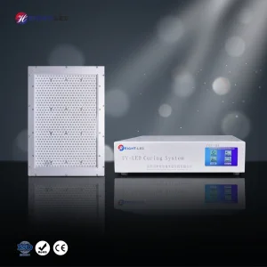
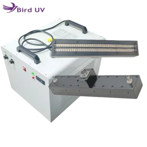
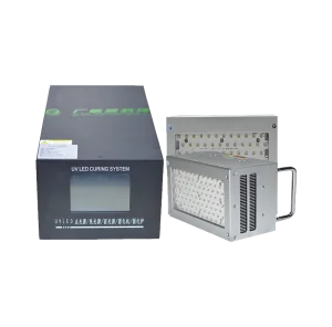
Explore our advanced product range, featuring water-cooled curing arrays, cleanroom wafer degummers, and lab-scale weathering equipment.
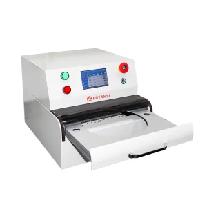
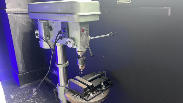
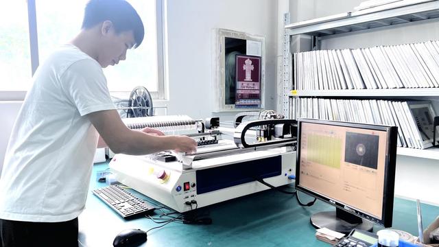
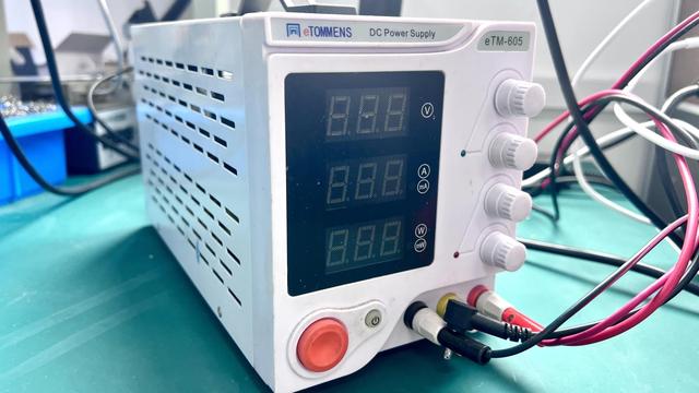
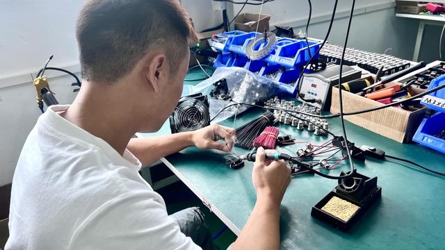
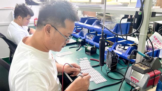
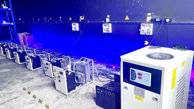
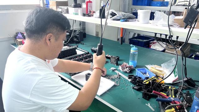
Review our advanced manufacturing facilities, optical testing stations, and integrated product quality verification processes.
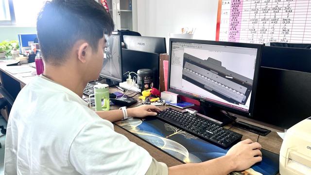
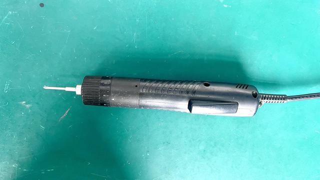
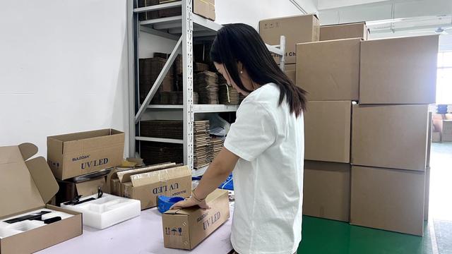
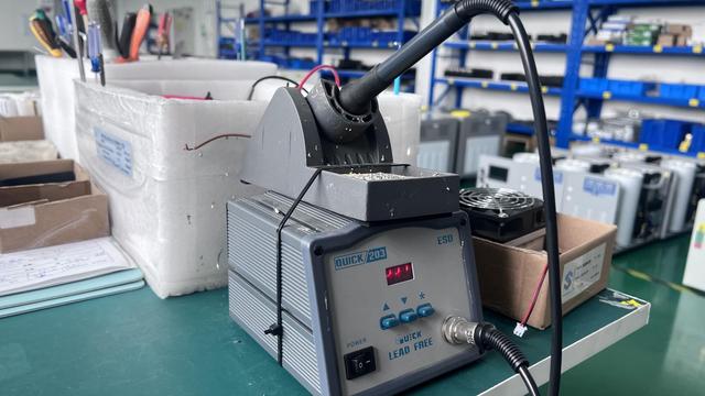
Our team of engineers can help customize wavelengths, sizing, cooling methods, and N2 purging capabilities to meet your specific requirements.
 LumiCure Light